The Dutch Giant Behind India's First Chip Fab
In this story
Every chip in your phone, your car and your laptop was drawn with light. The machines that do that drawing are some of the most complex ever built, and almost all of the advanced ones come from a single Dutch company: ASML. So when Tata Electronics announced in May 2026 that ASML would support its fab in Dholera, it was far more than a routine supplier deal. The Tata ASML partnership links India’s first commercial 300mm chip plant to the heart of the global semiconductor industry.
Why should a Dholera land owner, or anyone watching Gujarat, care about lithography? Because a chip fab is only as good as the tools inside it. Big announcements are easy. Getting the world’s most in-demand machines installed, tuned and running on time is hard. This partnership is about exactly that.
So what does ASML actually bring to Dholera, and how does it change the timeline?
A quick recap. Tata Electronics is building a 300mm (12-inch) semiconductor fab in Dholera Special Investment Region, with a planned investment of about US$11 billion, or roughly ₹91,000 crore. The process technology is licensed from Taiwan’s PSMC, covering nodes from 28nm to 110nm. At full production, the fab is designed to process up to 50,000 wafers a month, making chips for cars, mobile devices, AI systems and communications.
Reports in May 2026 put civil construction at around half complete, with trial production targeted for late 2026. The fab site was also designated a Special Economic Zone in April 2026. In other words, the building is rising. Now it needs its most important machines.
What the Tata ASML Partnership Covers
Announced on 16 May 2026, the Tata ASML partnership goes well beyond selling machines. According to the joint announcement, ASML will:
- Supply lithography tools and solutions: its holistic suite of equipment and software for patterning chips.
- Support fab set-up and ramp-up: helping the plant move from installation to steady production.
- Train local talent: building lithography skills among Indian engineers.
- Develop R&D infrastructure: supporting research capabilities in India.
- Strengthen supply chains: improving the resilience of parts and service support.
Tata Electronics CEO and MD Dr Randhir Thakur said ASML’s expertise in holistic lithography solutions will ensure the timely ramp of the Dholera fab. ASML President and CEO Christophe Fouquet said the company is committed to long-term partnerships in the region and to helping nurture talent in India. You can read the full ASML press release.
What is lithography, in plain English?
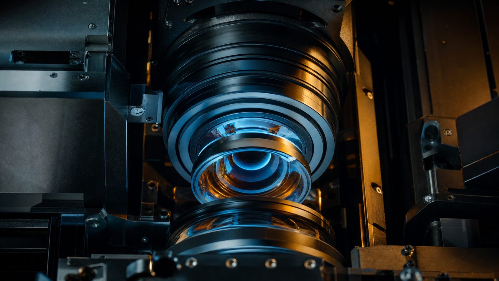
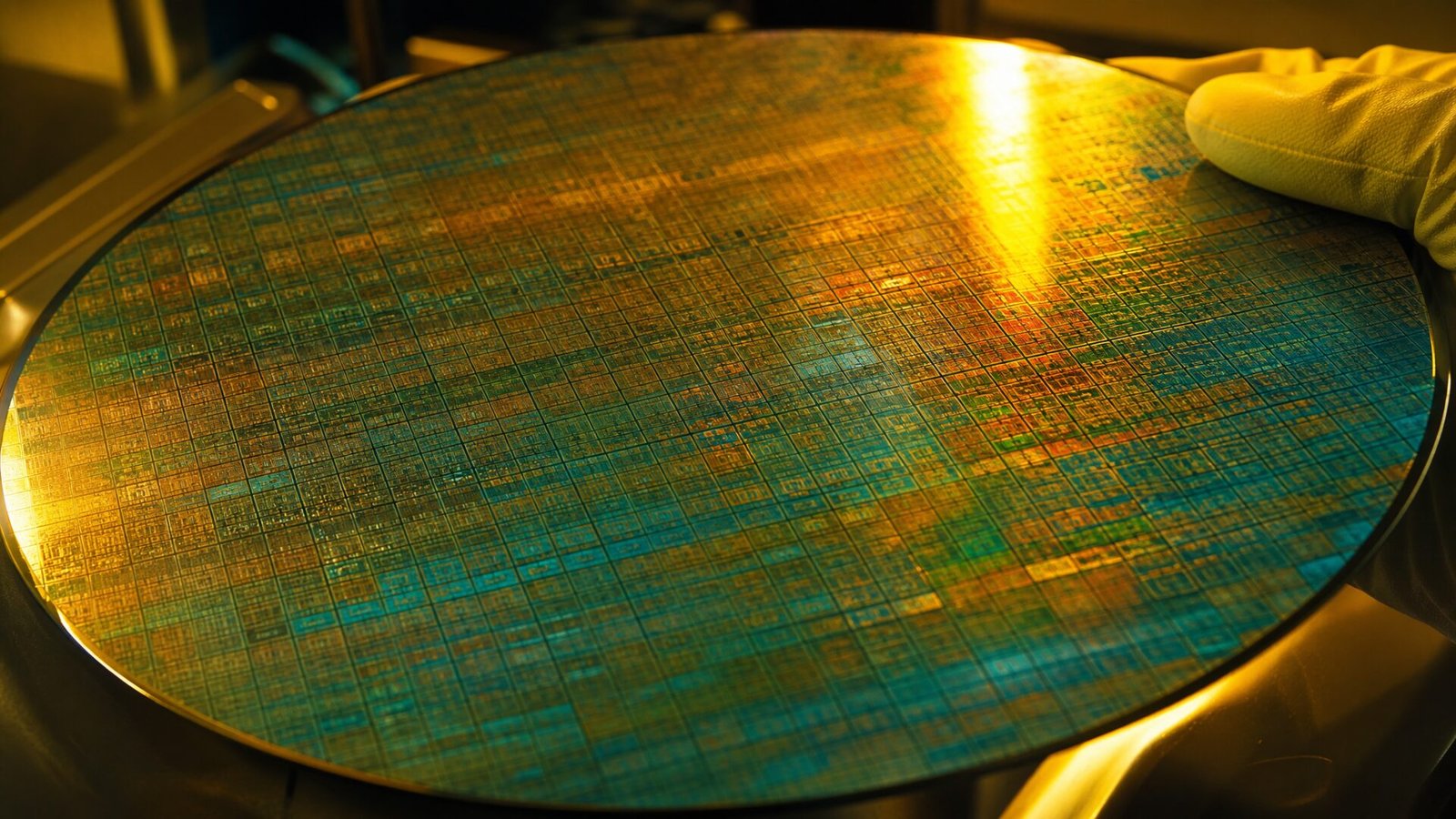
Think of it as ultra-precise photography. Light is shone through a pattern onto a silicon wafer coated with a light-sensitive chemical. Where the light lands, the chemical changes, and that pattern becomes the blueprint for billions of tiny transistors. Repeat this dozens of times, layer by layer, and you have a chip. The scanners that do it must line up each layer to within a few nanometres, which is why so few companies can build them.
Why ASML is so hard to replace
ASML, based in the Netherlands, is the world’s leading maker of lithography systems and the only company that builds the most advanced extreme ultraviolet (EUV) machines. Its deep ultraviolet (DUV) scanners are also the workhorses of fabs making the kinds of mature and mid-range chips planned for Dholera. Each scanner is the size of a bus, contains tens of thousands of parts and needs specialist engineers to install and maintain.
That’s why the Tata ASML partnership is about people as much as machines. Having ASML engineers involved during set-up, and training Indian teams to run and service the tools, is what keeps a fab running smoothly year after year. Under the Tata ASML partnership, that knowledge starts to build up inside India rather than being flown in each time something needs fixing.
Why the Tata ASML Partnership Matters So Much
In a fab, lithography is the critical path. It decides how many wafers you can process, how small your circuits can be and how many chips come out working. That’s why the Tata ASML partnership is such an important signal:
- Speed: direct support from the tool maker shortens the time from installation to production.
- Quality: well-tuned scanners mean higher yields, which is what makes a fab profitable.
- Credibility: global customers look at who equips a fab before they place orders.
- Skills: training Indian engineers on the world’s most advanced tools builds long-term capability.
It also fits a pattern. Back in September 2024, Tata Electronics signed a strategic partnership with Japan’s Tokyo Electron for fab equipment and training. Step by step, the world’s leading tool makers are lining up behind Dholera.
The Road to First Wafers
A 300mm fab moves through clear stages before it ships a single chip:
- Construction: cleanroom buildings, utilities and support systems.
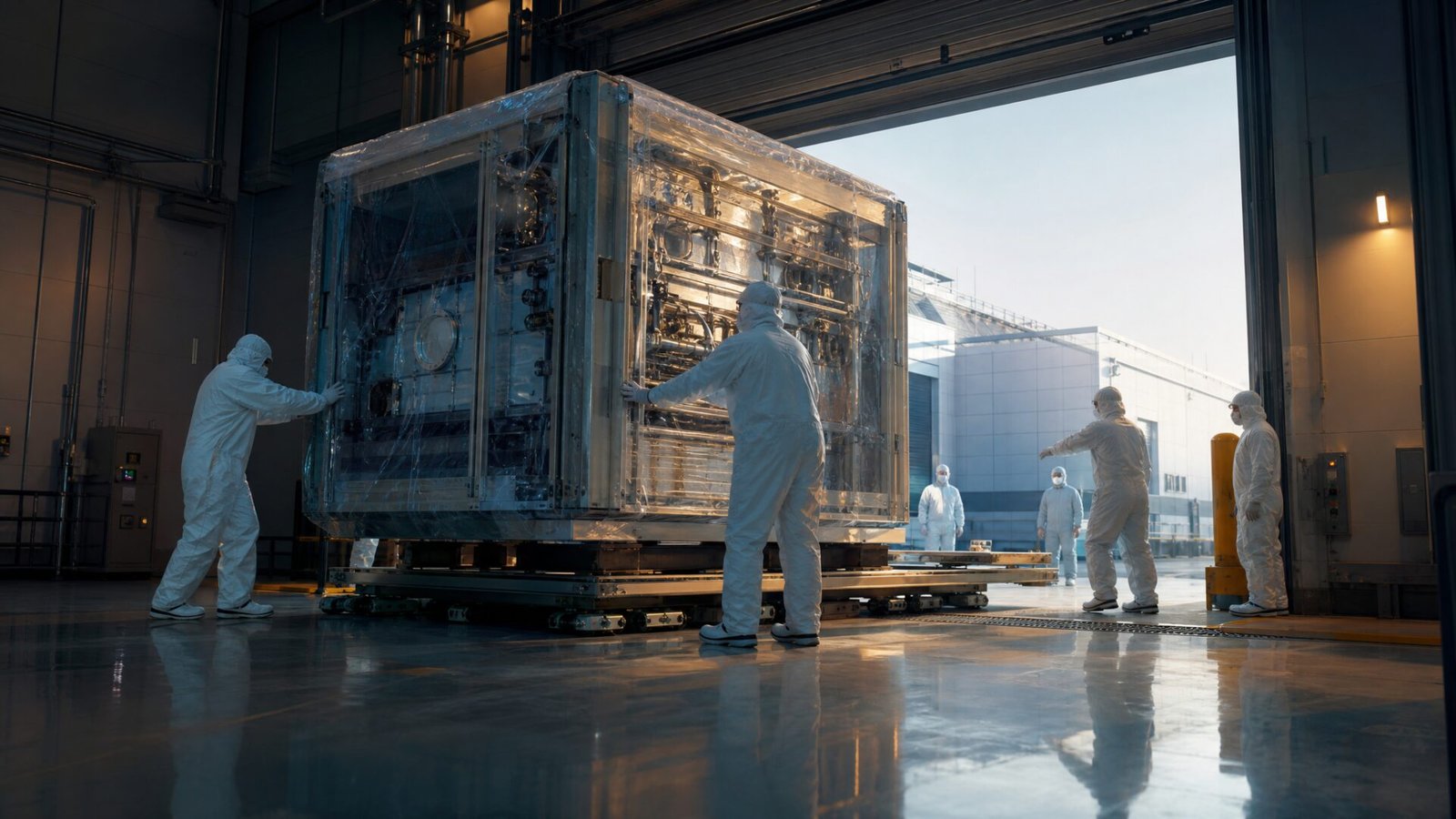
- Tool move-in: hundreds of machines arrive, with lithography scanners among the most delicate.
- Installation and qualification: each tool is connected, calibrated and tested.
- Trial production: first wafers are run and yields are tuned.
- Volume ramp: output climbs toward full capacity.
The Tata ASML partnership targets the middle of this journey, where fabs most often lose time. That’s why industry watchers see it as one of the most practical steps yet toward Dholera’s first chips.
For comparison, new fabs around the world often take two to three years to go from groundbreaking to first production, and the tool installation stage alone can take many months. Having the tool maker closely involved is one of the best ways to keep that stage on track. It also reduces the risk of costly delays once expensive machines are on site, because problems can be solved with the people who designed the equipment.
The Indian government's role
The fab is backed by the India Semiconductor Mission, which reportedly covers around half of eligible project costs. That kind of support gives companies like ASML the confidence to commit people and resources for the long term, rather than treating India as a one-off order.
Tata ASML Partnership: What to Watch Next
If you want to follow the Tata ASML partnership like an insider, watch for these milestones over the coming months:
- Tool move-in: news of lithography scanners and other key equipment arriving at the Dholera site.
- Hiring and training: programmes for Indian engineers on ASML and other fab tools.
- Trial wafers: the first test runs, which reports have targeted for late 2026.
- New suppliers: chemical, gas and parts companies setting up near the fab.
Each of these turns the Tata ASML partnership from a signed agreement into working capacity. And each one moves Dholera a step closer to becoming a real semiconductor city rather than a promise on paper.
What the Tata ASML Partnership Means for Dholera
For Dholera, the chip fab is the anchor tenant, and every step that brings it closer to production strengthens the whole city. A working fab means thousands of direct and indirect jobs, a steady flow of engineers and suppliers, and growing demand for homes, schools, shops and services.
- Jobs: engineers, technicians, maintenance teams and service staff.
- Suppliers: companies that provide gases, chemicals, parts and services tend to cluster near fabs.
- Housing: skilled workers and their families need places to live close by.
- Reputation: a fab equipped by ASML puts Dholera on the global semiconductor map.
For land buyers, the lesson is to follow real milestones like this rather than hype. Look for approved, clear-title plots with good access to the SIR, the expressway and the upcoming airport, such as Gulfin Aerocity near Pipli junction. As always, returns depend on market conditions, so do your own research.
The Bottom Line
Buildings can be rushed. Tools cannot. By bringing ASML directly into the project, Tata has tackled one of the hardest parts of building a fab. The Tata ASML partnership doesn’t just add a supplier. It adds the one company every serious chipmaker in the world depends on. For Dholera, that’s a very good sign.
We share updates on Dholera’s chip story on LinkedIn and Instagram.
Keep an eye on this space. As tools arrive and trial wafers begin, we will cover each step and what it means for Dholera’s growth, jobs and land market.
Tata ASML Partnership: FAQs
What is the Tata ASML partnership?
Announced on 16 May 2026, it is a strategic partnership under which ASML supports Tata Electronics’ Dholera fab with lithography tools and solutions, fab ramp-up support, talent training, R&D infrastructure and supply chain resilience.
What will the Dholera fab produce?
It is a 300mm fab using 28nm to 110nm process nodes licensed from PSMC, making chips for automotive, mobile, AI and communications applications.
How big is the Dholera chip fab?
It has a planned investment of about US$11 billion (roughly ₹91,000 crore) and is designed for up to 50,000 wafers a month at full production.
When will the Dholera fab start production?
Reports in May 2026 pointed to trial production targeted for late 2026, with volume production ramping up after that.
How does this affect Dholera real estate?
Milestones that bring the fab closer to production support jobs and housing demand, but price growth is never guaranteed. Check approvals and access before buying land.
Follow Gulfin Developers
Site walkthroughs, Dholera updates and new launches, first on our channels.
Recent Posts