Phase 1 vs Phase 2: Fujifilm's Dholera Game Plan
In this story
Big industrial projects rarely arrive all at once. They are built in steps, each one matched to demand. That’s exactly how Fujifilm is approaching Dholera. Rather than building every product line on day one, the Fujifilm Dholera plant is planned in two phases: first the chemicals a new chip fab needs most urgently, then the more specialised materials that follow as production scales up.
Why should anyone outside the chip industry care about phases? Because phased plans tell you how serious and how realistic a project is. They show what will happen first, what depends on what, and roughly when the real impact on jobs and land will arrive.
So what’s in each phase, and what does the timeline look like?
A quick recap. In September 2026, Fujifilm and Tata Electronics announced a strategic partnership, including an MoU for Fujifilm to invest about ₹800 crore, in phases, in a semiconductor materials plant in Dholera SIR, near Tata’s ₹91,000 crore chip fab. Read the full breakdown in Fujifilm just bet ₹800 crore on Dholera, and why the two are linked in Chips vs Chemicals.
Later reporting, including by Business Standard, added detail on how the plant will roll out.
Phase 1 of the Fujifilm Dholera Plant: Front-End Process Chemicals
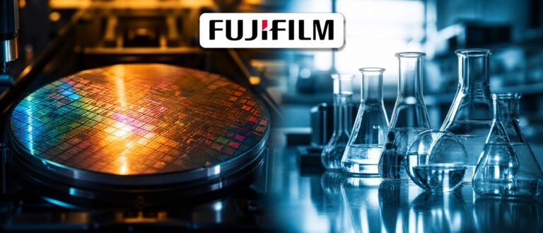
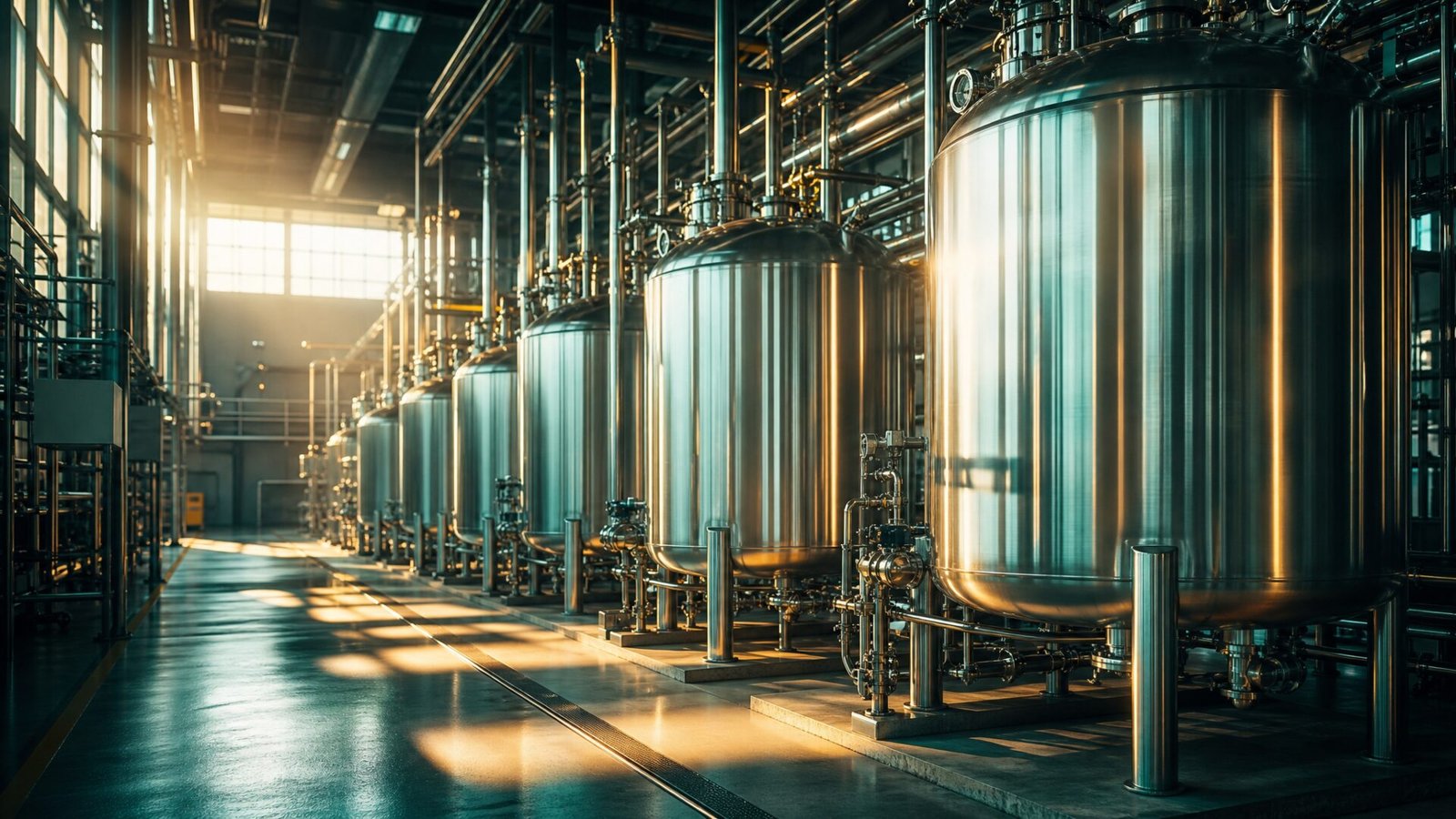
The first phase focuses on front-end process chemicals: the materials used while circuits are being built on the wafer. These include chemistries used in cleaning, patterning and etching steps, which a fab consumes continuously from the moment it starts running.
- Why first: these are the materials a new fab needs from day one.
- Main customer: Tata Electronics is described as an important customer at the initial stage.
- Timeline: commercial production is targeted for 2027–28.
- Sourcing: key raw materials are expected to be imported at first, with local sourcing growing over time.
Starting here makes sense. It lines up Phase 1 of the Fujifilm Dholera plant with the Tata fab’s ramp from trial production toward volume output.
What "front-end" means
Chipmaking has two big halves. Front-end work builds the tiny circuits on the wafer, layer by layer, inside the fab. Back-end work cuts the wafer into individual chips, packages them and tests them. Front-end processing uses the widest range of ultra-pure chemicals, which is why it’s the natural starting point for a materials supplier.
How Phase 1 lines up with the Tata fab
Timing is everything in a supply chain. Reports have pointed to trial production at the Tata fab starting around the end of 2026, followed by a gradual ramp toward full output. The Fujifilm Dholera plant’s Phase 1 target of 2027–28 fits neatly into that curve. In the fab’s early months, when volumes are low, imported chemicals can fill the gap. As production grows and consumption rises, locally made front-end chemicals from the Fujifilm Dholera plant can take over more of the supply.
That hand-over is a common pattern in new chip regions. Suppliers rarely start at full scale on day one. They grow alongside their customer, learning its processes and tuning products to its tools. Being next door makes that learning much faster, which is one of the biggest advantages of the Fujifilm Dholera plant’s location.
Phase 2: Surface Conditioning and High-Purity Materials
The second phase adds semiconductor surface conditioning materials and high-purity chemicals. Surface conditioning refers to the materials used to polish and clean wafer surfaces between steps, such as CMP (chemical mechanical planarisation) slurries and post-CMP cleaners. These steps keep each layer perfectly flat and spotless so the next layer can be built on top.
- Why second: these materials become more critical as the fab runs more complex process flows at higher volumes.
- Higher value: advanced polishing and cleaning materials are highly specialised and need tight quality control.
- Wider customer base: by this stage, Fujifilm aims to serve more than one fab or packaging unit in India.
Why phasing reduces risk
Building a full materials plant before the customer’s fab is running would be risky and expensive. Phasing lets Fujifilm invest step by step, matching production to real demand, testing quality with Tata, and training local staff and partners along the way. It’s the same logic the Tata fab itself follows: trial production first, then a gradual ramp toward full capacity.
Building quality from day one
For semiconductor materials, quality is everything. Each batch must match strict purity and performance specifications, and fabs test incoming materials carefully before using them. The Fujifilm Dholera plant will need clean production areas, advanced analytical labs and highly trained staff to meet those standards. Building this capability step by step, starting with Phase 1, gives the team time to prove its processes with Tata before expanding into the more demanding Phase 2 materials.
Beyond Tata: Fujifilm's Bigger India Plan
Fujifilm India MD Koji Wada has said India is looking to significantly expand semiconductor manufacturing and that the company expects more front-end manufacturing facilities to come up. He also described a plan to partner with Indian companies, guide them with manufacturing and technical know-how, support them with technology transfer and eventually buy from them.
- More customers: future fabs and packaging companies across India.
- Local partners: Indian chemical makers trained to semiconductor-grade standards.
- Deeper supply chain: gradually replacing imported raw materials with local ones.
In other words, the Fujifilm Dholera plant is meant to be a hub for India’s wider chip industry, not just a single supply line to one fab.
Why India needs local semiconductor materials
Today, India imports almost all of the specialised materials its electronics industry uses. That leaves chipmakers exposed to shipping delays, currency swings and global shortages. A domestic supply of semiconductor materials would make Indian fabs more resilient and more competitive. The Fujifilm Dholera plant is one of the first serious steps toward that goal, and its success could encourage other global materials companies to build in India too.
It also matters for skills. Making semiconductor-grade materials requires expertise in chemistry, process control and quality testing that India is still building. Every phase of the Fujifilm Dholera plant adds to that knowledge base, training people who could one day lead India’s own materials companies.
The Fujifilm Dholera Plant Timeline at a Glance
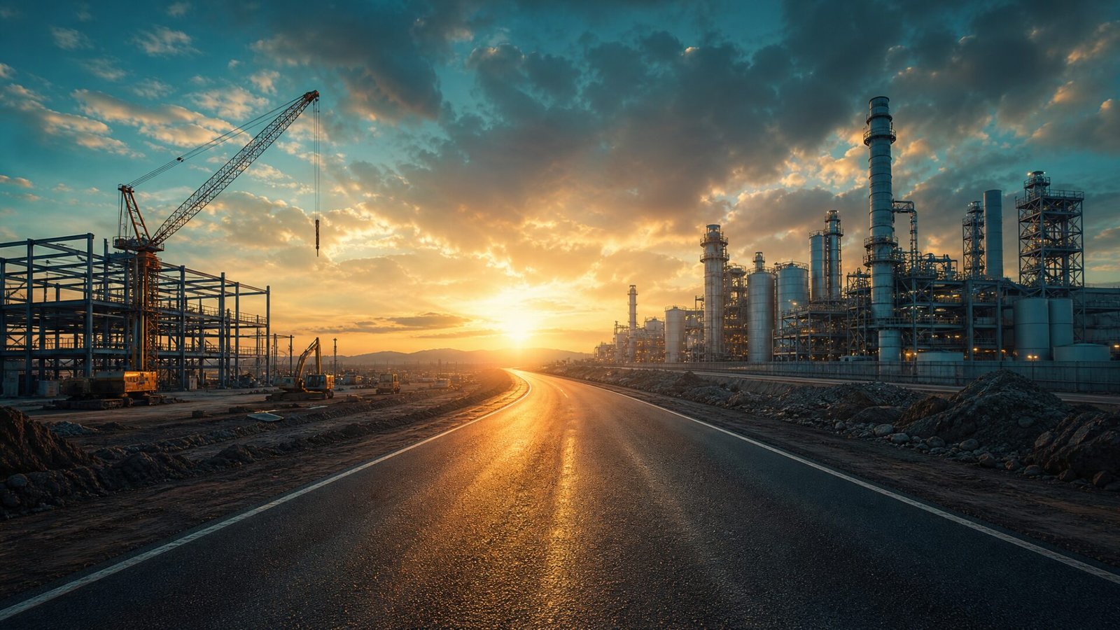
- September 2026: Fujifilm and Tata Electronics announce their partnership and the ₹800 crore MoU.
- Next steps: land allotment, detailed design and construction in Dholera SIR.
- 2027–28: targeted start of commercial production for Phase 1, front-end process chemicals.
- Later: Phase 2 adds surface conditioning materials and high-purity chemicals as demand grows.
As with any industrial project, dates can shift. But the structure is clear, and it lines up well with the Tata fab’s own ramp-up.
What Each Phase Means for Dholera
Each phase brings its own ripple effects:
- Phase 1: construction jobs, then chemists, process engineers, lab and safety staff; early demand for industrial land and staff housing near the fab.
- Phase 2: more specialised roles, more suppliers and a stronger case for other materials and gas companies to join the cluster.
- Across both: technology transfer that helps Indian companies move up the value chain.
For land buyers, that points to steady, gradual demand rather than a sudden jump. Approved, clear-title land with good access to the SIR, the expressway and the airport, such as Gulfin Aerocity near Pipli junction, is best placed to benefit. As always, returns depend on market conditions.
Signals to track
Watch for land allotment and groundbreaking for the Fujifilm Dholera plant, updates on the Tata fab’s trial production, announcements of Indian partner companies, and any news of other materials or gas suppliers following Fujifilm. Together, they will show how fast Dholera’s chip cluster is growing.
One Step at a Time
Great industrial clusters aren’t built in a day. They’re built phase by phase, customer by customer, supplier by supplier. The Fujifilm Dholera plant follows that proven path: front-end chemicals first, surface conditioning and high-purity materials next, and a growing network of Indian partners throughout. If it stays on track, 2027–28 could be the moment Dholera’s chip story truly becomes an industry.
We share semiconductor updates on LinkedIn, Instagram and YouTube.
Fujifilm Dholera Plant: FAQs
What will Phase 1 of the Fujifilm Dholera plant produce?
Front-end process chemicals, the materials used while circuits are built on the wafer, with Tata Electronics as an important early customer.
What is in Phase 2?
Semiconductor surface conditioning materials, such as CMP slurries and cleaners, plus high-purity chemicals.
When will the Fujifilm Dholera plant start production?
Commercial production is targeted for 2027–28, according to reports following the announcement. Timelines may change.
How much is Fujifilm investing in Dholera?
About ₹800 crore (roughly US$83 million), in phases, under an MoU with Tata Electronics announced in September 2026.
Will Fujifilm supply companies other than Tata?
Yes, the plan is to serve other future fabs and packaging companies in India as the market grows.
Follow Gulfin Developers
Site walkthroughs, Dholera updates and new launches, first on our channels.
Recent Posts